RL Circuit Simulation
Overview
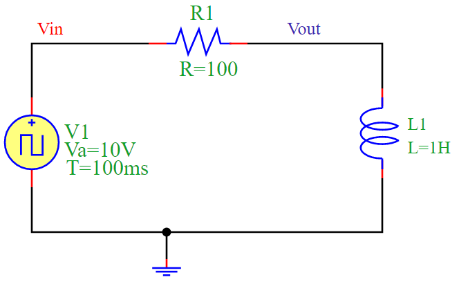
The circuit consists of a resistor (R1) and an inductor (L1) forming an RL circuit. The circuit is driven by a square wave voltage source (V1).
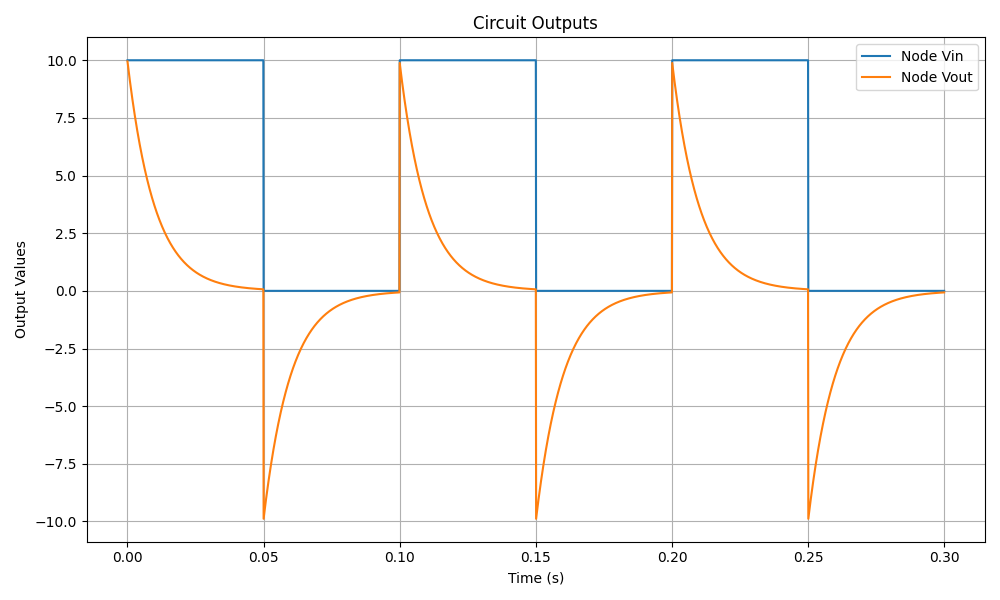
When the input voltage Vin switches from low to high, the inductor L1 resists the change in current, causing a gradual increase in current through R1.
When Vin switches from high to low, the inductor resists the decrease in current, resulting in an exponential decay of current through R1.
This creates a characteristic exponential response to changes in voltage.
Time Constant
The time constant (τ) of an RL circuit is given by:
For this simulation:
Resistance: R = 100 Omega
Inductance: L = 1H
Time Constant: τ = 1 / 100 = 0.01 s
Circuit Diagram
The following diagram illustrates the RL circuit:
Simulation Output
The output voltage Vout follows an exponential response due to the inductor’s resistance to changes in current. The simulation produces the following waveform:
Conclusion
The RL circuit demonstrates inductive behavior, where the inductor resists changes in current, causing a smooth exponential rise and fall. This behavior makes RL circuits useful in applications such as filtering, signal processing, and energy storage.